Layer 1
An optically transparent interface layer designed to modify band bending and increase useful built-in potential.
The technology
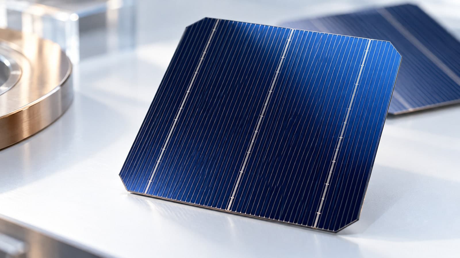
We are developing a dual-layer p-type contact for n-type TOPCon cells. Our objective is to recover voltage at the front interface while retaining the manufacturing architecture.
The interface opportunity
The contact between metal and p-type silicon can create an electronic barrier. Our contact architecture is intended to improve band bending, reduce losses and support charge collection.
Conventional TOPCon
The front contact can contribute to barriers, recombination and resistive losses.
SiVolt contact concept
Designed to improve the front electrical interface while preserving the core cell architecture.
Conceptual architecture; layers are not to scale. Detailed materials and process parameters are available through confidential technical diligence.
An optically transparent interface layer designed to modify band bending and increase useful built-in potential.
An optically transparent, conductive layer intended to support the interface and provide lateral charge transport.
Our proposed retrofit directly substitutes conventional AlOₓ/SiN front layers, preserving the dominant steps of the underlying TOPCon manufacturing sequence.
Reported evidence
Laboratory testing on a 20-cell sample reports improvements in voltage, current and fill factor.
Reported laboratory resultOur approximately 27% cell-efficiency endpoint is a development target. Performance must be independently replicated on industrial-format wafers, at commercial throughput and acceptable yield.
Development targetExplore the validation milestonesEquipment integration
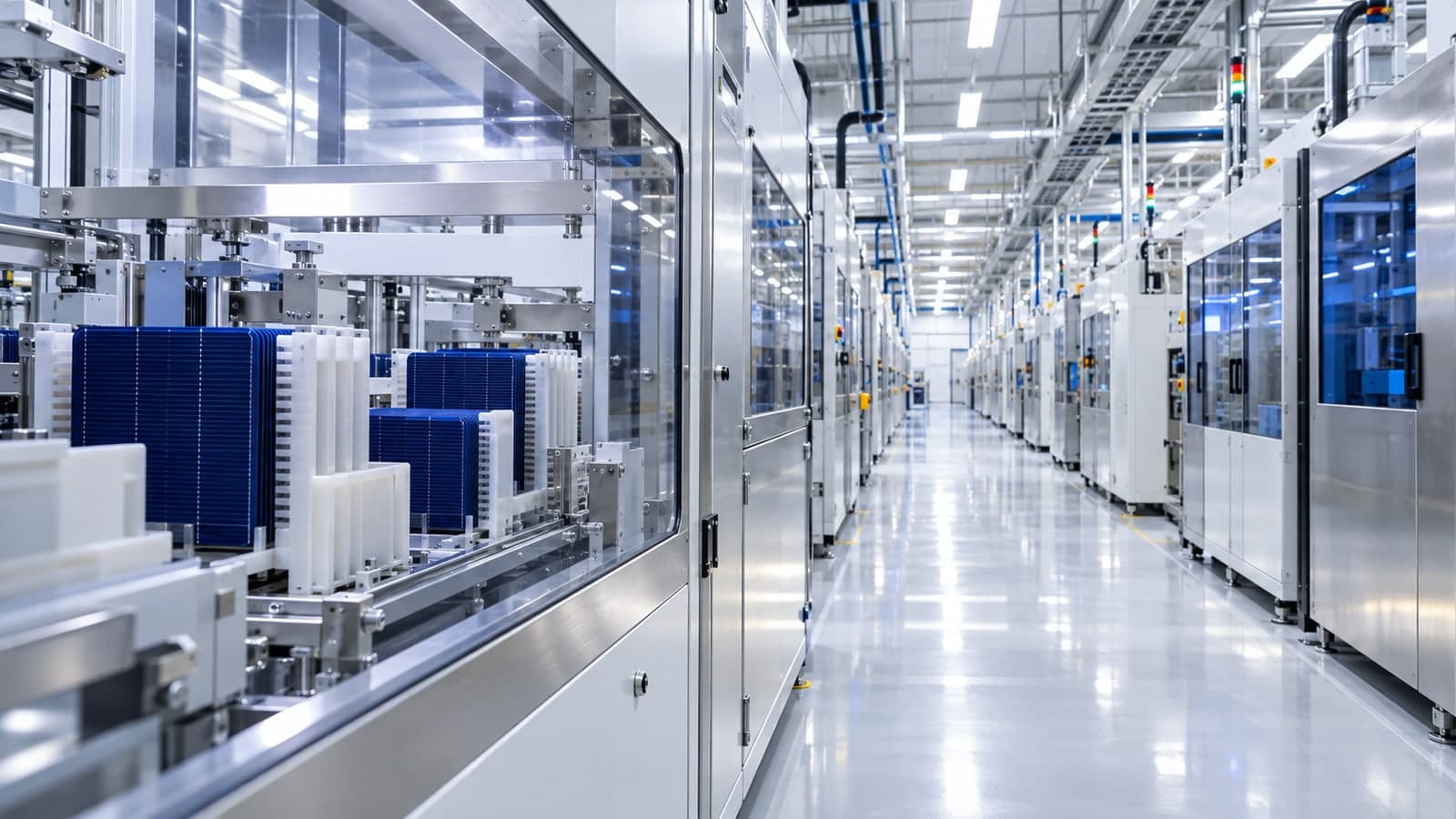
Our intended process uses two deposition steps. Existing tool reuse and process integration remain subject to technical confirmation.
VON ARDENNE has been identified as the primary equipment integration candidate in our engineering evaluations. Its TOPCon coating equipment provides relevant industrial context.
Candidate European equipment ecosystem
| Equipment supplier | Country |
|---|---|
| VON ARDENNE | Germany |
| SPTS / KLA | United Kingdom |
| Evatec | Switzerland |
| Singulus | Germany |
| IHI / Hauzer | Netherlands |
Equipment compatibility and commercial agreements remain subject to validation and confirmation.
The next conversation